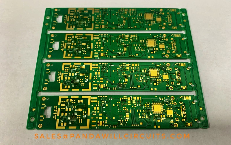
HDI PCB is multilayer boards with a higher connection pad density than standard boards, with finer lines/spaces, smaller via holes and capture pads allowing microvias to only penetrate select layers and also be placed in surface pads.
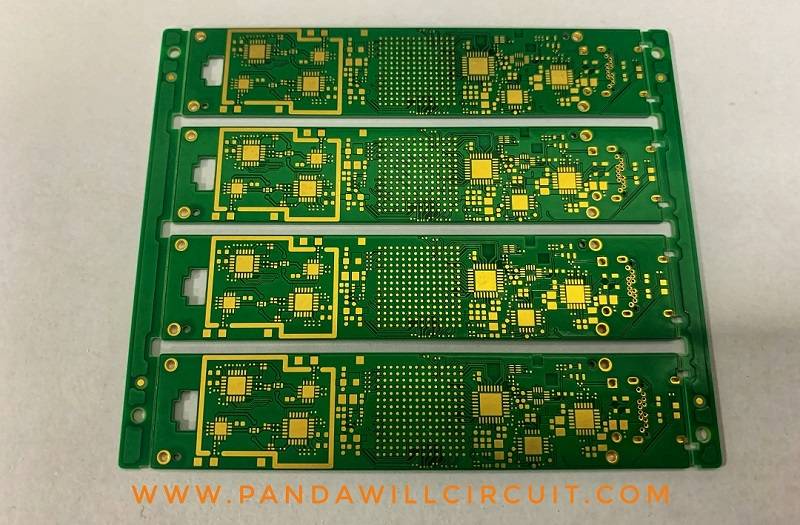
HDI any-layer printed circuit boards are the next technological enhancement of HDI microvia printed circuit boards: all the electrical connections between the individual layers consist of laser-drilled microvias. The main advantage of this technology is that all the layers can be freely interconnected. To produce these circuit boards, Pandawill uses laser-drilled microvias electroplated with copper.
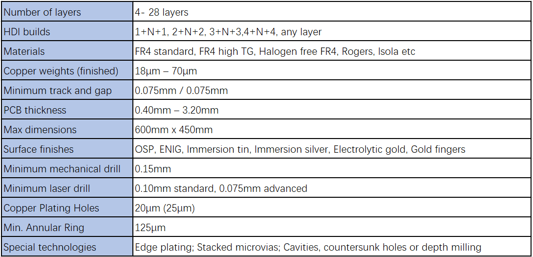
Pandawill Circuits HDI PCB Technical Specifications:
Pandawill Circuits has a long experience building HDI boards, with a team of engineers with a deep expertise producing HDI PCBs for different market applications. Please contact our sales at sales@pandawillcircuits.com if you need further information or assistance, we are happy to help you.